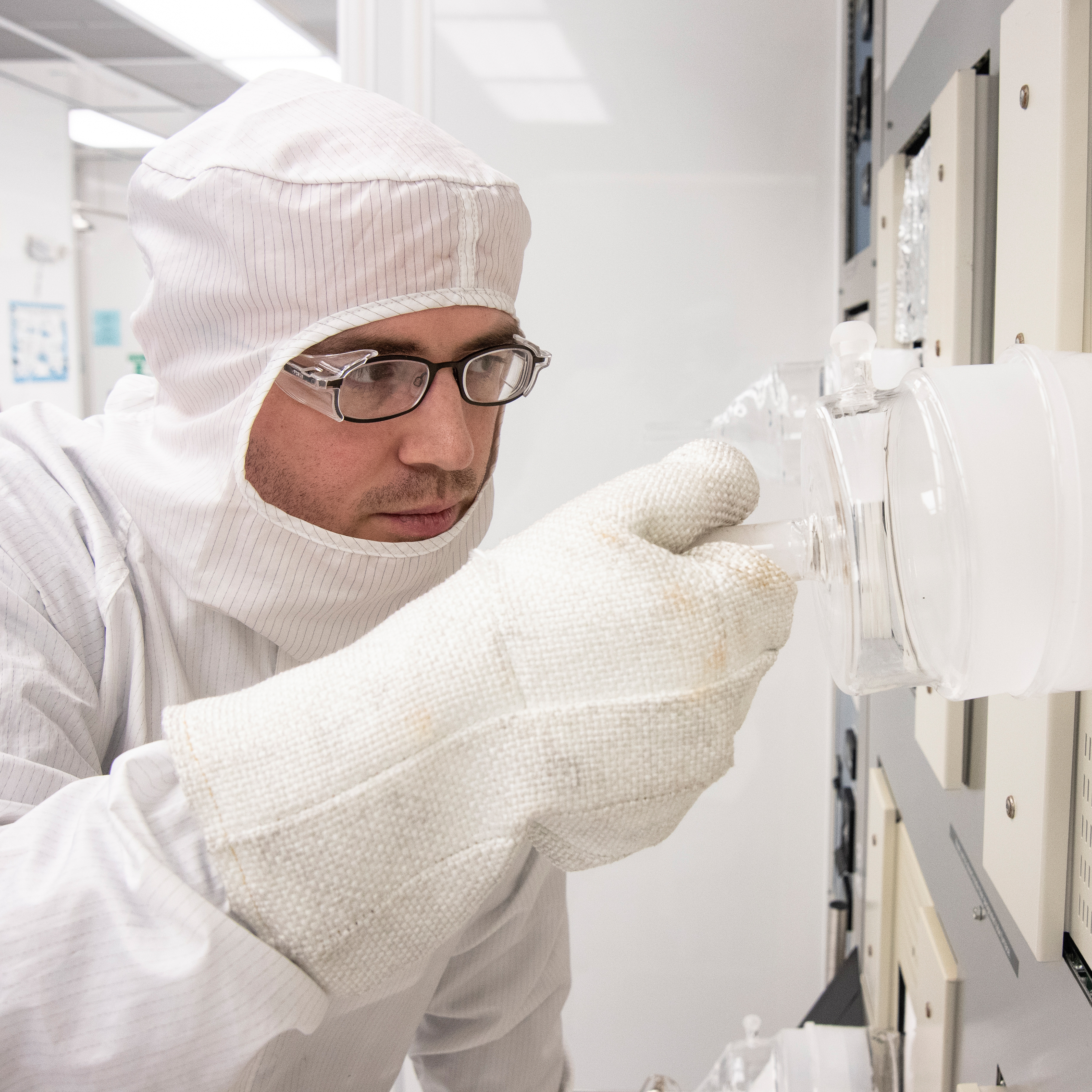
The Thermal Bay is where all of our high temperature processes take place. A silicon wafer can conduct electricity for it is naturally a semiconductor. This can be a problem if we place designs on the surface of the wafer for they may short circuit or electrically connect through the wafer when we don’t want them to. In order to address this problem, we can grow a film on the surface of the wafer that does not conduct electricity. For silicon wafers this thin film is called silicon dioxide or SiO2. It won’t conduct electricity and is similar to glass. Silicon dioxide is grown by placing clean wafers in a furnace at very high temperatures like 1000°C or 1832 F along with high purity oxygen. The end result is that oxygen atoms bond with silicon atoms to form silicon dioxide, which slowly grows as a thin film on the surface of the wafer.

