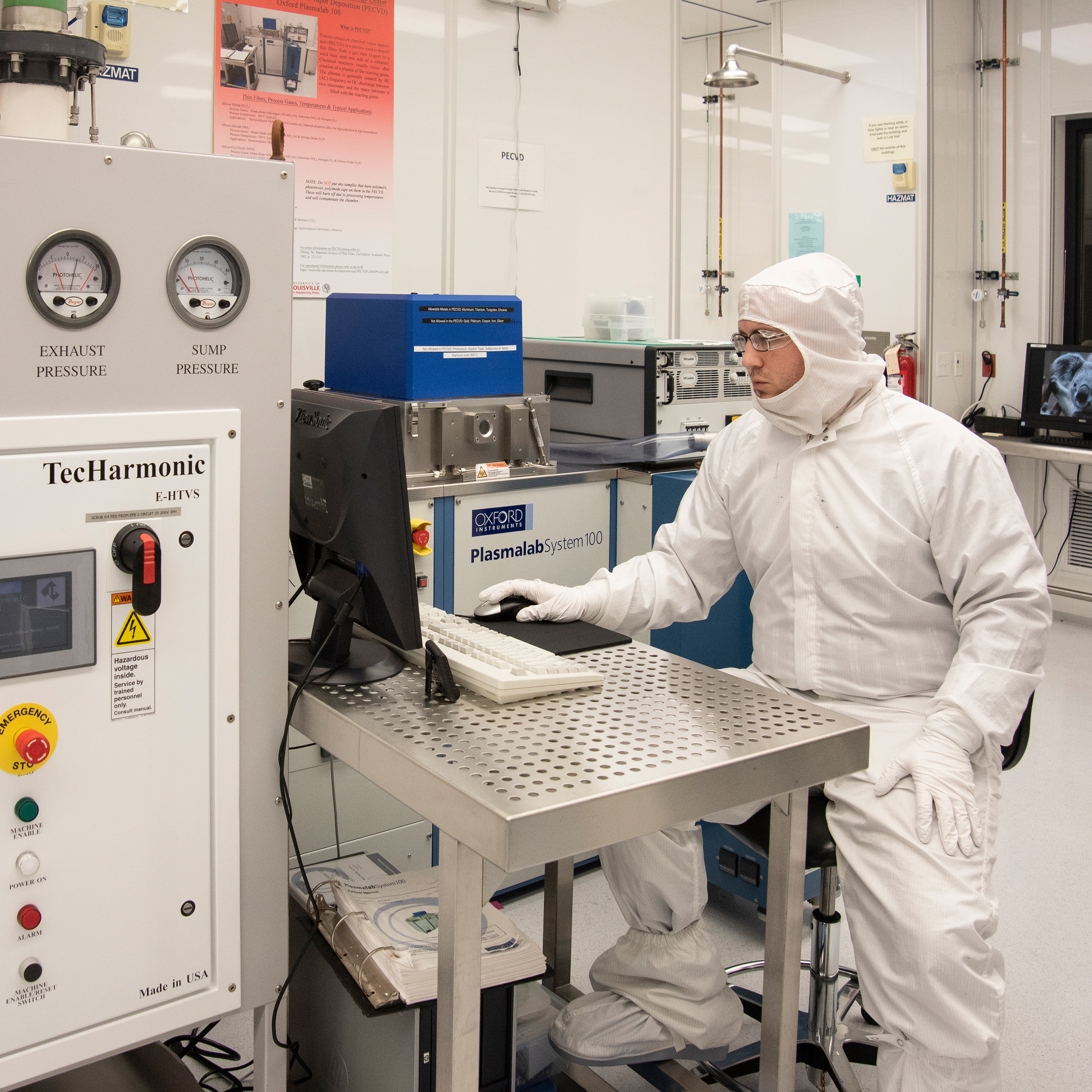
Within the deposition bay we perform the crucial step of depositing many different materials onto the wafer. These materials can vary from precious metals like gold and platinum, common metals like copper and nickel or materials totally unlike metals that do not conduct electricity. There are several types of deposition methods depending on the process requirements.
Sputtering is the most common form of deposition performed in our cleanroom. During this process, both the wafer and the material to be deposited are under high vacuum. Plasma, which is similar to lightning or the glow from neon signs, is used to carve out and eject microscopic particles from the target to land on the wafer. This process allows for deposition of very thin nanometer layers.
Other processes in our cleanroom include plasma enhanced chemical vapor deposition, electron beam evaporation, atomic layer deposition and molecular vapor deposition. These processes are described in more detail on our deposition self-guided tour page. The next step on your self-guided tour is photolithography, which is near the end of the cleanroom and is easy to find due to its orange colored rooms.