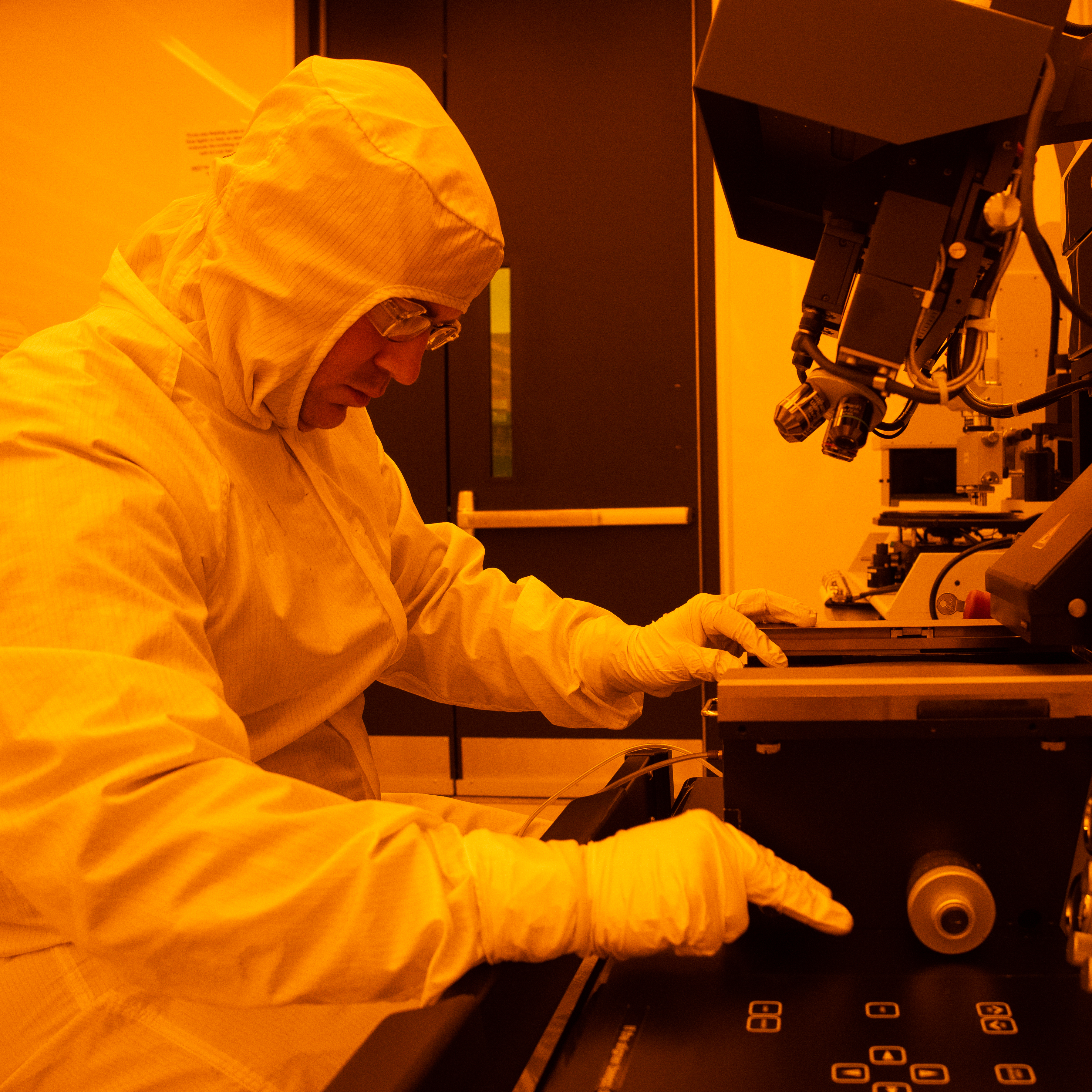
After a thin film has been deposited onto the wafer it is now time to take the next steps to make the deposited layer into a design. A stencil is applied to the wafer, so we can etch away the deposited material we don’t want to keep. Photolithography is the process of making the stenciled design onto our wafer. This process is similar to using a negative made by a camera with a roll of film to make a picture. Negatives used in the cleanroom are made of glass and have a chrome metal pattern on them like you see in the window. Instead of printing onto paper to make a picture we use special liquid polymers called photoresist that are spun onto the wafer. These polymers have chains that react when exposed to a special wavelength of UV light. After exposure to the UV light the wafer is placed in a developer solution. Areas exposed to the UV light will have broken chains and wash away. Areas that were protected by the chrome and not exposed will cross-link and form the desired pattern onto the wafer. Using these steps we can generate patterns as small as 4 micrometers. You may also be asking why the bay is orange. The reason for this color is that all UV light which is close to blue light has been removed. This safeguard ensures we do not accidentally expose and activate our expensive photoresist and gives the bay its orange color.